The next step is to create the Technology Layers in the template file. The final version of the template file contains a total of seven Metal Technology Layers and six Via Technology Layers. Similar to the dielectric layers, you will only create some of the Technology Layers to save time then continue the tutorial with a partial template that contains all of the Technology Layers.
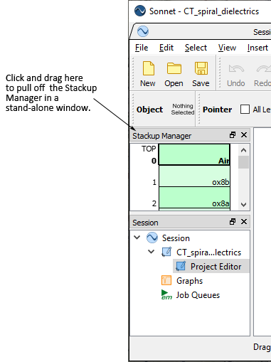
This file should be available in the working directory where you saved the example files. This is a template file which contains the complete dielectric stackup. Note that in order to see the whole stackup, you will more than likely need to "pull off" the Stackup Manager into a separate window and resize it (shown below) so that the dielectric names are displayed. If you do not wish to expand the size, you can use the scroll bars to the right and bottom of the stackup to access all of the dielectric levels.
Next, you will add a “Metal6” and “Metal5” Metal Technology Layer and a “Via5” Via Technology Layer that extends between them to your template.
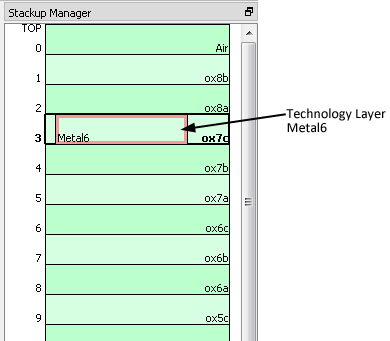
The Technology Layer dialog box appears on your display. You clicked on “ox7c” dielectric layer since the “Metal6” Technology Layer needs to be assigned to metal level 3. In Sonnet, metal levels are associated with the dielectric layer above them, and added metal always extends upwards. It is possible to edit the level number in the Technology Layer dialog box, but by selecting this dielectric layer, the metal level defaults to the desired value.

The name of the Metal Technology Layer will be Metal6. The level is already the correct value as discussed above, so you do not need to change it.
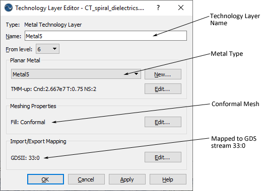
The metal type which you wish to use for this Technology Layer is not yet defined in this project. Clicking on the New button opens the Planar Metal Editor dialog box. For more information on planar metal types and how they are modeled, please see Planar Metalization Loss in the Sonnet User's Guide.
It is not necessary to use the Technology Layer name as the metal type name, but it is often convenient. This is the name of the metal type you are creating.
This metal is a thick metal, and this model allows you to model the metal as possessing an actual physical thickness, instead of normal metal, which is modeled as a 2D sheet.
You may define the loss of your metal using Conductivity, Resistivity or Sheet Resistance at DC. For more information, please see Conductivity. Resistivity or Sheet Resistance at DC in the Sonnet User's Guide.
Metal6 is a 3.0 micron thick metal. The default value of two sheets is appropriate and does not need to be changed. The dialog box should look like the picture shown below. Notice that a new pattern has been automatically assigned to this metal type. This pattern can be used to easily identify the metal type when editing your circuit. You can choose any pattern.
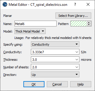
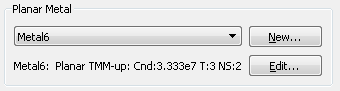
The Planar Metal section of the Technology Layer dialog box is updated with information about the new metal type. The parameters of the metal are displayed beneath the name; “TMM-up” stands for Thick Metal Model that extends upward from level 3.
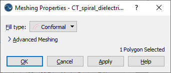
This metal is going to be used for a polygon with diagonal edges. Conformal mesh is more efficient with polygons with curved or diagonal edges, so you need to change the meshing properties of this Technology Layer. Conformal Mesh in the Sonnet User’s Guide.
The Meshing Properties dialog box is opened on your display.
This sets the fill type to Conformal for the Technology Layer. Any polygon associated with the Technology Layer will use conformal mesh.
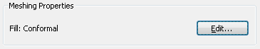
The Meshing Properties section of the Technology Layer dialog box is updated.
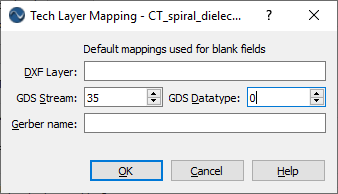
The Import/Export Mapping dialog box is opened on your display. This dialog box allows you to map a GDSII stream and datatype to the Technology Layer. When that GDSII stream is imported, the objects in it will be added to the Technology Layer. You will be mapping GDSII stream 35:0 to this Technology Layer.
The entries for the DXF Layer and Gerber Filename can be left empty as they are ignored when importing a GDSII file.
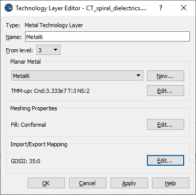
The Technology Layer dialog box is updated and should now appear as shown below.
The Stackup Manager is updated with the Metal6 Technology Layer. Note that the Technology Layer is shown as only a red outline since there are no polygons assigned to it. Red is used to represent Metal Technology Layers in the Stackup Manager. It is also drawn as the same height as the dielectric to indicate that it is a thick metal which is the same thickness as the dielectric layer above it; both the dielectric layer ox7c and metal type Metal6 are 3.0 microns thick. If it had been a thick metal that was thinner than the dielectric layer, it would be drawn to cover only half the dielectric layer.
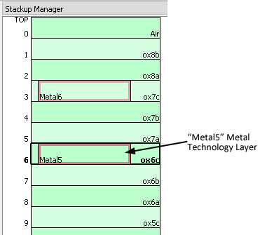
Note that this will also require creating a new planar metal type also named “Metal5.” The properties for the metal type are Thick Metal Model, a conductivity of 2.667e7 S/m and a thickness of 0.75 microns.
The stackup should now appear as follows:
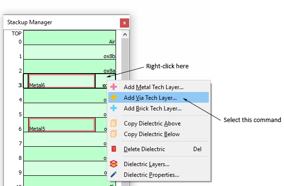
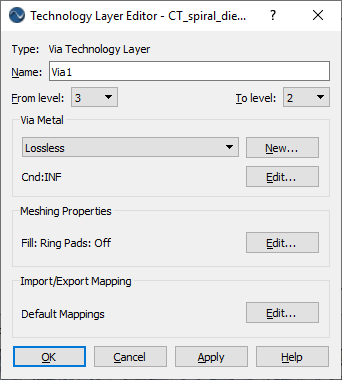
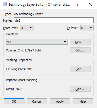
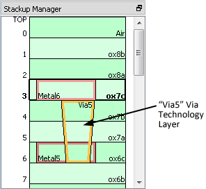
Now you will add the Via Technology Layer Via5 to the template. The Via5 Via Technology Layer extends between the Metal6 and Metal5 Technology Layers.
The Technology Layer Editor dialog box appears on your display. Note that the type is a Via Technology Layer.
The Via Technology Layer will be displayed as Via5 in the Stackup Manager.
Note that the From Level is set to level 3, which is the location of the Metal Technology Layer from which you selected the Add Via Tech Layer command.
The From and To level drop lists each contain all the levels defined in the project. Note that there is no difference between a via which goes from level 3 to level 6, and a via which goes from Level 6 to level 3; both would provide the same electrical results. Entering 6 for the From level and 3 for the To level would have resulted in the same Via Technology Layer.
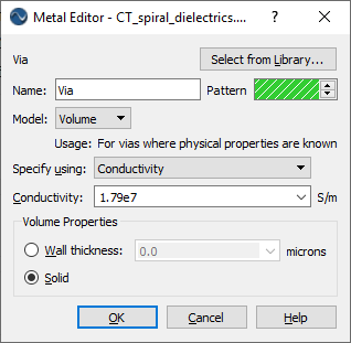
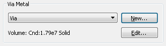
The Via Metal Editor dialog box is opened. If a metal which you wished to use was already defined, you would select it from the drop list. Since there are no via metal types defined in the project aside from the default Lossless, you will need to create the via metal type for this Technology Layer.
The via metal type you are creating will be named Via. We are using only one via metal type in this template project so we will not use the default name.
This models the vias as solid and the complete area of the via polygon is used for the loss calculations. For more information on via metal types and how they are modeled, please see Via Metalization Loss in the Sonnet User's Guide.
The Technology Layer dialog box is updated.
The default meshing properties do not need to be changed.
The Import/Export Mapping dialog box appears on your display.
The DXF Layer and Gerber Filename entries may be left blank since they are ignored when importing a GDSII file.
The Technology Layers dialog box is updated and should appear as shown below.
The Stackup Manager is updated and now displays the “Via5” Via Technology Layer. The Via5 technology layer symbol is shown unfilled in yellow. Yellow is used to represent Via Technology Layers in the Stackup Manager. This Technology Layer symbol is unfilled because it has no objects assigned to it. If polygons are created using a Technology Layer then the symbol appears in the Stackup manager as filled.
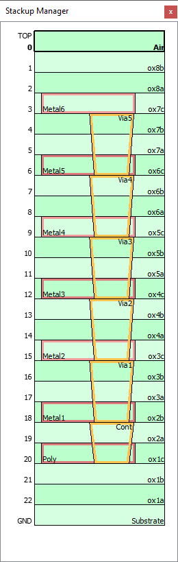
This completes the Technology Layers you will create in this tutorial. To continue, you will open a partial template that contains the entire dielectric stackup and all of the Technology Layers and material properties.
This closes the file. A query appears to ask about the changes you have made; click on Discard.
This file should be available in the working directory where you saved the example files. This is a template file which contains the complete dielectric stackup and all Technology Layers, as shown below.