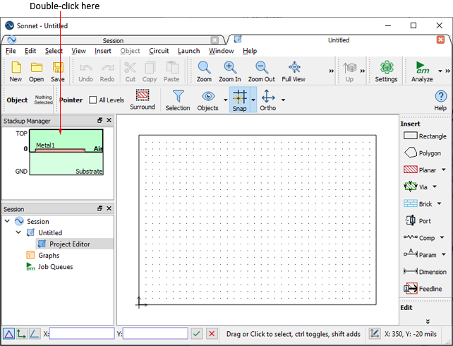
Next, we will set up the dielectric stackup. This information is usually provided by your foundry or fabrication vendor. Some vendors do not include an air layer on top, but if your circuit is to be used in air, you should always add a thick layer of air to the top of your stackup. You will edit one of the existing dielectric layers, then add a new dielectric layer. The rest of the dielectric stackup is supplied in a partial template provided with your example files.
 Instead of manually creating the whole template project, you may also set up your dielectric stackup by importing a Sonnet substrate file, created in the Cadence Virtuoso Interface or Keysight ADS Interface, using the Circuit ⇒ Load Technology command in the project editor. The Interfaces can be used to convert other technology files to a Sonnet substrate file.
This top layer will be the thick layer of air at the top of the stackup.
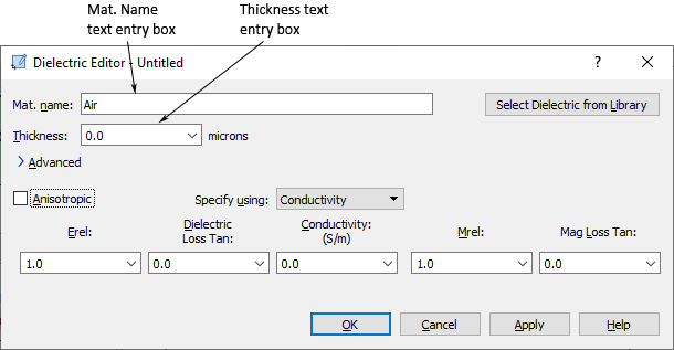
The Dielectric Editor dialog box appears on your display.
You could also have left the Circuit Settings dialog box open, and clicked on "Dielectric Layers" in the side bar menu. When the Dielectric Layers are displayed, you would select the top row, then click on the "Edit" button to open the Dielectric Editor dialog box.
This defines a 5000 micron layer of air at the top of your stackup. The rest of the parameters, including the material name, are correct for air, so no further editing is required.
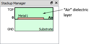
The appearance of the Stackup Manager is not changed since the default name of the dielectric layer was air and the height of the dielectric layer does not change as the stackup manager is not to scale.
Now you will add a new dielectric layer to the stackup.
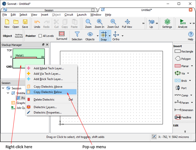
A new "Substrate" dielectric is added to the bottom of the stackup. Now that you have created a new dielectric layer, we will define its properties.

The Dielectric Editor appears on your display.
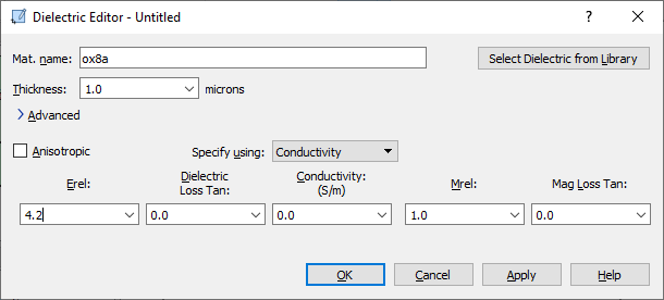
The dialog box should appear as shown below. This will create a 1.0 micron thick dielectric layer named ox8a whose relative dielectric constant is 4.2.
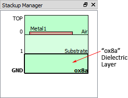
The stackup manager now displays “ox8a” as the dielectric name.
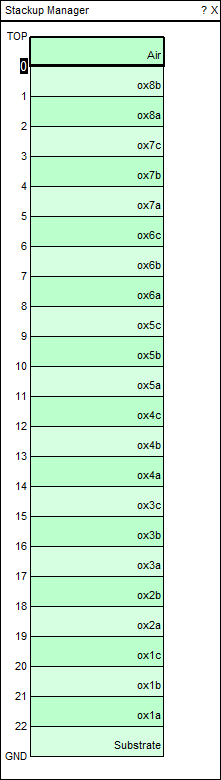
This completes the dielectrics you will edit and create in this tutorial. To continue, you will open a partial template that contains the entire dielectric stackup. The entire stackup is shown below.
This closes the file. A query appears to ask about the changes you have made; click on Discard.